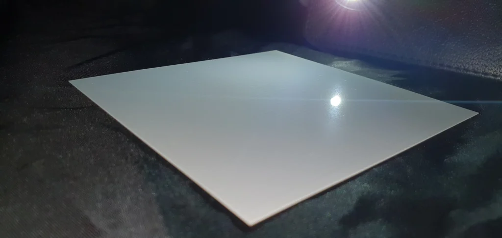
Keral 99 TF
The big advantage of this alumina substrate is the very smooth surface due to the fine-grained structure of < 2µm particles. Our Keral 99 TF was developed primarily for thinfilm applications and can be easily cut or structured by using a laser or wafer saw. The deposition of platinum is easily realized with the usual thinfilm technology. Thanks to the advantageous evenness of
< 200µm (4″ x 4″), fine conductive circuits are precisely mapped. The substrates are “Made in Germany” here in Eschenbach i.d.OPf. We cut the material according to your requirements using laser equipment. Please send us your CAD data.

Advantages
from KERAL 99 TF
- Very fine-grained, homogeneous grain structure 2 µm
- Good electric insulation properties
- High bending strength > 500 MPa
- Processing by laser or wafer saw possible
- Excellent price-performance ratio
- Smooth surfaces for fine structures Ra<90nm
Applications
Keral 99 TF
- Thinfilm application, e.g. temperature sensors